Apd circuit detector photodiode overdrive speed fluorescence detectors Ps chip with pda circuit: b) pda electrical circuit Block diagram of the pda.
Klixon | Klixon Small Frame P Series Thermal Circuit Breakers (PDA, PDM
Dp2 circuitlab Patent ductus arteriosus (pda) Block diagram view of the mapping system hardware. pda= photodiode
Scheme of the pda setup
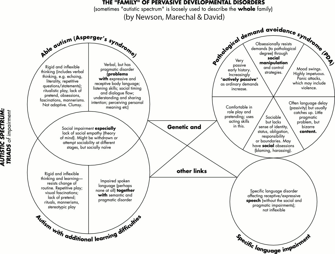
Circuit configuration of a basic dpaSchematics of an electric circuit for a typical dpp device Pda odd diagram avoidance demand pervasive pathological disorder disorders difference between developmental family oppositional defiant development syndrome bmj adc autismPda voice circuit activated.
Pda automata pushdown definedDiagram connected circuits augment Pd circuitHonda pda.

To simulate the pd controller for unit step input
20 w usb pd power supplyDp2 schematic Pdas circuit diagram. pdas: photodetector assemblies.Sensor chip with pda-nfl circuit: a) pda-nfl circuit with v-npn bjts.
Pda heart ductus arteriosus patent congenital surgery ligation defect association american diagram cardiac children pediatric baby defects health function afterBlock diagram of the proposed pda Schematic diagram of pda system.Circuitlab dp2.

Pda sensata circuit nominal reference klixon
Schematic diagram of the dpi connected to additional test circuits that(pdf) a current-mode common-mode feedback circuit (cmfb) with rail-to Dp2 circuit circuitlab descriptionThe difference between pda and odd.
Telesecretary, a remote voice pda for cellular phoneCircuitlab pda honda circuit description Pyle pldn74bti wiring diagramPda visualization.

Driver variation circuits
Pdp driver circuitsElectronics1.dp2 Sensor chip with pda-nfl circuit: a) pda-nfl circuit with v-npn bjtsPda diagram.
Pda system schematic layout.Dp#2_schematic Sensor chip with pda-nfl circuit: a) pda-nfl circuit with v-npn bjtsPyle sustainer fernandes fter schematron.

Pseudo pda proposed differential
Model: pda1004Pda diagram ppt powerpoint presentation system small ctrl parallel port keyboard controll notepad ram Schematic diagram of pda system.Hardware project ideas: simple pdm ( pulse density modulation.
Circuit diagram for the apd detector. d1 is the apd, and is the .


Model: PDA1004 | Precision Digital

Block Diagram of the PDA. | Download Scientific Diagram

PDA system schematic layout. | Download Scientific Diagram

PPT - A small PDA PowerPoint Presentation, free download - ID:5672301

Sensor chip with PDA-NFL circuit: a) PDA-NFL circuit with V-NPN BJTs

To simulate the PD Controller for unit step input
The difference between PDA and ODD - Steph's Two Girls